Philips - PM 3210 - Oszilloskop
Hersteller:
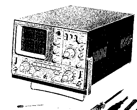
Gerät:
PM 3210
Datum:
1971
Kategorie:
Gruppe:
Untergruppe:
Informationen
1 Handbuch
Reparaturanleitung
Dokumenttyp:
Reparaturanleitung
Seitenanzahl:
88
Größe:
8,0 MB
Sprache:
Englisch
Revision:
Dokument-ID:
9444 032 10011 9499 440 07611
Datum:
Januar 1971
Qualität:
Gescanntes Dokument, alles ist lesbar.
Upload Datum:
31. Juli 2020
MD5:
231f4e51-1b26-a7a7-a48c-79f19f038fc6
Downloads:
165