Fluke - PM3392A - Oscilloscope
Manufacturer:
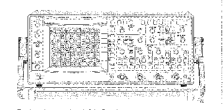
Image 1 of 3
If you have any other photos or manuals for the
Fluke PM3392A
you can
upload the files here.
Equipment:
PM3392A
Date:
1994
Category:
Group:
Sub Group:
Information
There are four models in this family of Fluke oscilloscopes.
Each of these models is a combination of an analog real-time
oscilloscope and a fully featured digital storage
oscilloscope. By pressing a single push button, you can
switch the instrument from the analog mode to the digital
mode and back. This allows each of the units to be used in
an optimum operating mode for all kinds of signal
conditions. Complex data streams, modulated waveforms, and
video signals can often best be seen in the analog mode of
operation. The digital mode of operation is more suited for
single events, signals with low repetition frequencies, and
when automatic measurements need to be performed.
In this family there is a choice of four models. Two models
have a bandwidth of 200 MHz; the two others have a bandwidth
of 100 MHz. There is a choice of two models with four fully
featured channels or four channels in a ’2+2’ configuration
In the same instrument family, there are two 200-MHz analog
oscilloscopes that have specifications similar to the
above-mentioned anaiog/digital combination oscilloscopes
operating in analog mode.
All analog/digital combination oscilloscopes listed above
have the following features:
- 8K sample acquisition memory, expandable to 32K.
- Up to 40 waveforms stored in memory or 204 waveforms with
optional memory extension.
- Autoset function for an instant optimized signal display
at the touch of a button.
- Auto-ranging attenuators.
- Auto-ranging timebase.
- Real time clock.
- Cursor measurements with 1 % accuracies.
Extensive set of fully automated voltmeter and time
measurement functions.
- Probe operated Touch Hold and Measure’ function freezes
the display and instantly displays the signal frequency,
amplitude and dc voltage level.
Peak detection for the capture of glitches as narrow as 5 ns.
- Pattern, State and Glitch triggering (2 ns)
- Event delay and pretriggering and posttiiggering.
- TV triggering including HDTV and TV line selection.
- Serial interface for printing and plotting.
- Averaging to reduce signai noise and to increase the
vertical resolution from 8 to 16 bits.
- Advanced mathematics, including digital Sow-pass
filtering. A Math+ option adds integration, differentiation,
histogramming, and (as part of a option) FFT.
- Sine interpolation and magnification which enables true to
life four channel single shot acquisitions with a timebase
up to 625 ns/div (32x magnified)
- A delayed timebase with full trigger features.
- An EIA-232-D interface (standard) and an GPiB/IEEE-488
interface (optional).
- Autocal for automatic fine tuning of all circuitry to
achieve maximum accuracy under all user conditions.
- Closed case calibration for efficient maintenance of
traceable calibration at minimum cost.
The following options are available:
- A MATH+ option with more automated measurement functions
including envelope and measurement pass/fai! testing. Aiso
included in this option are Integration, Differentiation,
Histogramming, and FFT,
- Memory extension offering 32K acquisition length and the
ability to store 204 traces (of 512 samples each) in memory.
IEEE-488.2 interface using the new SCPI (Standard Commands
for Programmable Instruments) industry standard for remote
control of test and measurement equipment.
3 Manuals
User manual
Manual type:
User manual
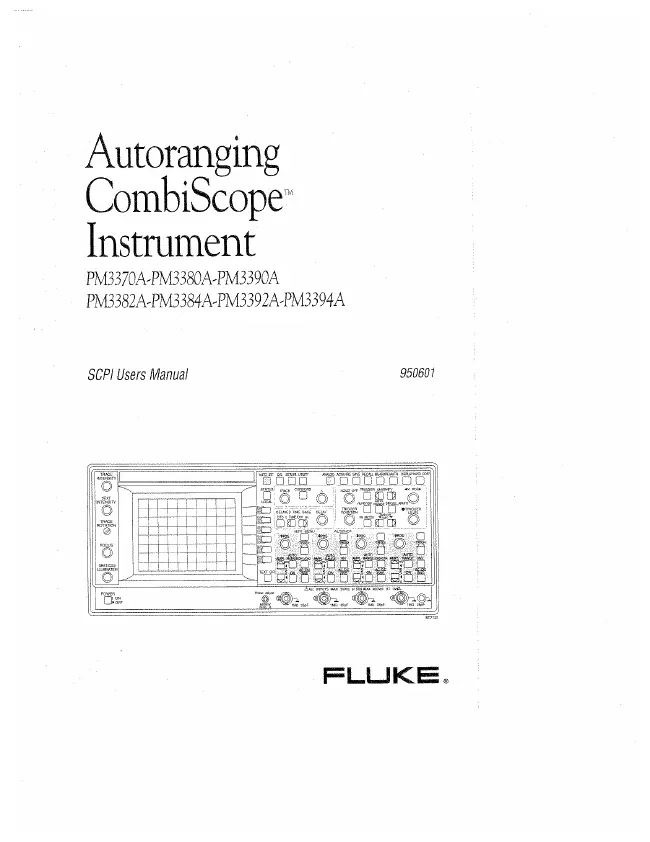
Pages:
304
Size:
8.1 MB
Language:
english
Revision:
Manual-ID:
950601
Date:
January 1994
Quality:
Scanned document, all readable.
Upload date:
Jan. 20, 2018
MD5:
1600b3ef-5e2a-4612-2622-4f2a59a954d4
Downloads:
4839
User manual
Manual type:
User manual
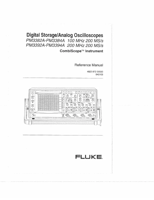
Pages:
128
Size:
3.5 MB
Language:
english
Revision:
Manual-ID:
4822 872 00583 940103
Date:
January 1994
Quality:
Scanned document, all readable.
Upload date:
Jan. 20, 2018
MD5:
7b2f794c-7e9a-569a-caf7-e4d8df589eec
Downloads:
2342
Service manual
Manual type:
Service manual
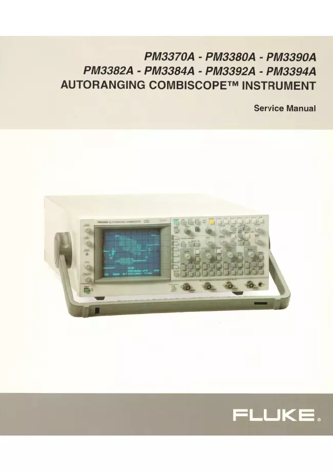
Pages:
473
Size:
9.1 MB
Language:
english
Revision:
Manual-ID:
4822 872 05366
Date:
June 1996
Quality:
Scanned document, all readable.
Upload date:
Jan. 20, 2018
MD5:
b6036e08-4816-062e-5b53-e83c44d67f5e
Downloads:
2462