Hitachi - VT-F551 E/F552E(VPS) - Video cassette recorder
Manufacturer:
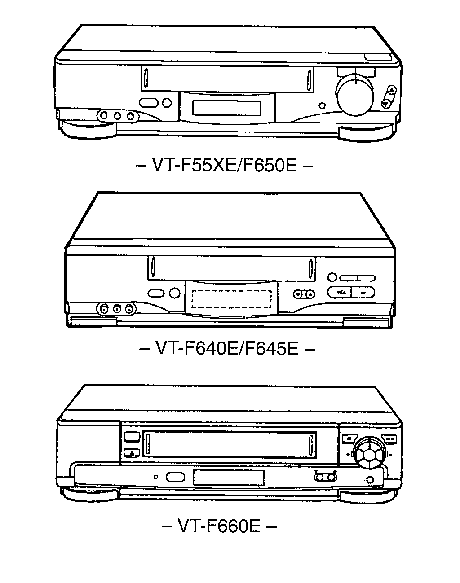
Image 1 of 1
If you have any other photos or manuals for the
Hitachi VT-F551 E/F552E(VPS)
you can
upload the files here.
Equipment:
VT-F551 E/F552E(VPS)
Date:
1997
Category:
Group:
Sub Group:
Information
1 Manual
Service manual
Manual type:
Service manual
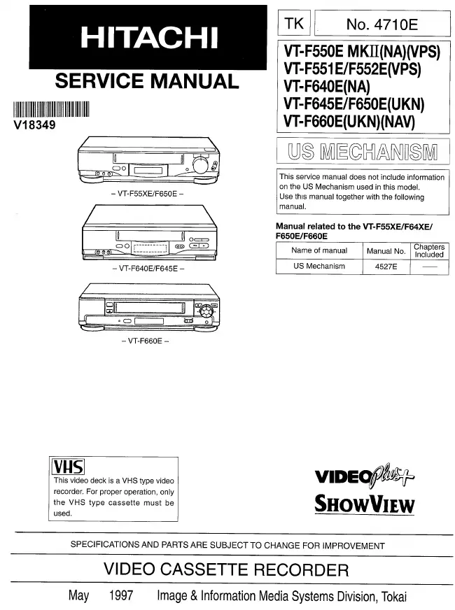
Pages:
90
Size:
8.9 MB
Language:
english
Revision:
Manual-ID:
4710E
Date:
May 1997
Quality:
Scanned document, all readable.
Upload date:
April 16, 2017
MD5:
12609b57-0fef-82c7-3bc8-e08cd2d577c9
Downloads:
1997