Philips - PM3217 - Oscilloscope
Manufacturer:
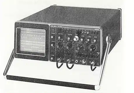
Image 1 of 5
If you have any other photos or manuals for the
Philips PM3217
you can
upload the files here.
Equipment:
PM3217
Date:
1981
Category:
Group:
Sub Group:
Information
50MHz dual channel analog oscilloscope.The 50 MHz dual-channel oscilloscope PM 3217 and PM 3217U is a compact, portable instrument, ergonomically designed to facilitate its extensive measuring capabilities.
The instrument provides both a main and a delayed timebase with provision for alternate timebase displays, comprehensive triggering facilities including peak-to-peak Auto, DC coupling and automatic TV waveform display.
A large 8 x 10 cm screen with illuminated internal graticule lines makes for easier viewing, and a 10 kV accelerating potential gives a high intensity trace with a well-defined spot.
The wide range of applications enabled by the above features is further extended by a versatile power supply that enables the instrument to be operated from different line voltages as well as from d.c. For field operation an optional battery version is also available.
3 Manuals
User manual
Manual type:
User manual

Pages:
44
Size:
6.4 MB
Language:
english
Revision:
Manual-ID:
9499 440 21501
Date:
October 1983
Quality:
Scanned document, all readable.
Upload date:
March 15, 2008
MD5:
8fa7abf8-5637-4e71-7dc4-5350bdc5ec36
Downloads:
4379
Service manual
Manual type:
Service manual
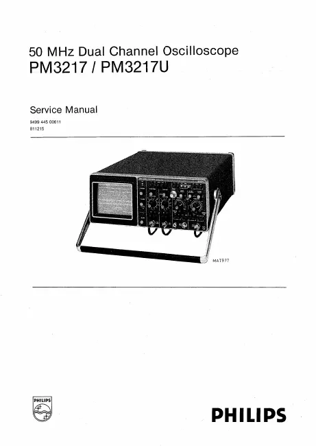
Pages:
160
Size:
18.2 MB
Language:
english
Revision:
Manual-ID:
9499 445 00611
Date:
December 1981
Quality:
Scanned document, all readable.
Upload date:
July 31, 2020
MD5:
42149fc3-b244-3826-b250-59bd49de1609
Downloads:
584
User manual
Manual type:
User manual
Pages:
108
Size:
15.8 MB
Language:
english, german, french
Revision:
Manual-ID:
9499 440 21501
Date:
October 1983
Quality:
Scanned document, all readable.
Upload date:
March 15, 2008
MD5:
53ecdfeb-2a20-4d42-ebf4-15996a19ab34
Downloads:
29