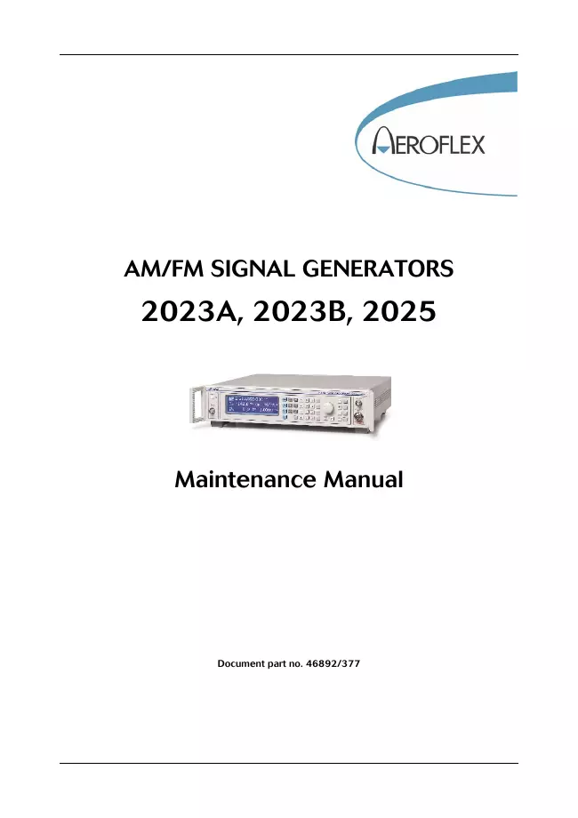
Aeroflex - 2025 - Generator
Manufacturer:

Image 1 of 1
If you have any other photos or manuals for the
Aeroflex 2025
you can
upload the files here.
Equipment:
2025
Date:
1999
Category:
Group:
Sub Group:
Information
Introduction
The 2023, 2023A, 2023B, 2024 and 2025 AM/FM Signal
Generators cover the following
frequency ranges:
9 kHz to 1.2 GHz 2023 and 2023A
9 kHz to 2.05 GHz 2023B
9 kHz to 2.4 GHz 2024
9 kHz to 2.51 GHz 2025
Output levels from -140 dBm to +13 dBm are available.
Factory fitted options are available to
extend the level to +25 dBm (+19 dBm above 1.2 GHz) and to
provide SINAD measurement
capability. Fig. 1-1 is a block diagram of the frequency
synthesis and signal processing circuits.
Synthesizer
A VCXO operating at 100 MHz is phase locked to the internal
(or external) frequency standard
using a phase comparator at 10 MHz. The VCXO signal is
divided by 20 to give a 5 MHz
reference frequency for the fractional-N loop phase comparator.
A fractional-N loop is used to lock a multiplied low-noise
VCO to the reference with a resolution
of l Hz. The VCO tunes from 400 to 535 MHz and is multiplied
by three, four or five to yield a
signal in the range 1.2 to 2.51 GHz. A high speed
programmable divider is used to divide the
multiplied VCO frequency down to 5 MHz and a phase
comparator compares this signal with the
reference derived from the VCXO. The output from the phase
comparator corrects the VCO
frequency. In order to provide the required division ratio,
the programmable divider is required to
act as a fractional divider. The fractional-N gate array
controls the division ratio of the
programmable divider. The variation of this division ratio
by the controller enables the loop to
lock, with non-integer division ratios, to the reference
with the resolution of 1 Hz without
introducing spurious signals.
FM is produced using a two-point modulation scheme. The FM
signal is inserted into the loop by
summing the FM signal with the VCO tune line to modulate the
VCO directly. Simultaneously,
the FM signal is fed to the fractional-N controller via a
1-bit oversampled A-D converter which
converts an analogue input into a bit stream of ‘1’s and
‘0’s. The controller uses this input to
modulate the division ratio in sympathy with the modulation.
This allows frequencies less than
the loop bandwidth, including DC, to modulate the output
frequency.
In order to maintain good FM performance of the two-point
modulation system, the VCO FM
tracking characteristics are required to be known. The
sensitivity of the FM system via the 1-bit
oversampled A-D converter is VCO independent and accurately
calibrated by a DC calibration
system. The VCO tracking is derived by an automatic FM
SELFCAL routine during calibration.
During an FM SELFCAL, the error signal on the tune line, for
a frequency near the loop
bandwidth, is monitored while varying the FM calibration
numbers, allowing the variation in VCO
sensitivities to be calibrated out. This will remove any
perturbation of FM flatness near the loop
bandwidth due to mismatch of two modulation paths.
RF processing
The VCO on board AA1 operates in the range 400 to 535 MHz
and feeds to a harmonic generator
whose 3rd, 4th and 5th harmonics are selected by
voltage-tuned band-pass filters to provide a
frequency in the range 1.2 to 2.4 GHz (2.51 GHz on board
AA1/1). To generate frequencies
below 1.2 GHz this signal is divided by factors of two to
produce frequencies in the range 10 MHz
to 1.2 GHz. A bank of switched half octave harmonic filters
follows which is used to reduce
unwanted harmonics at the output. Then the signal passes
through the amplitude modulator where
the output level envelope is controlled. The output from the
modulator is peak detected. For
frequencies less than 10 MHz the signal is mixed with an
input from the 100 MHz VCXO. The
resulting output in the frequency range 9 kHz to 2.4 or 2.51
GHz is fed from the output amplifier
to attenuator board AA2. For pulse operation the signal is
taken to the pulse modulator which
operates in the range 30 MHz to 2.51 GHz. Otherwise the
pulse modulator is bypassed and the
signal is fed to the output attenuator. This is controlled
by relays and provides attenuation in steps
of 11 dB up to 132 dB. The attenuator also includes an RPP
(Reverse Power Protection) system to
protect the instrument from accidental application of
reverse power.
LF processing
The LF processing all takes place on control board AB1 or
AB1/1, and may be conveniently
subdivided into the following major functional elements.
LF output
A DSP (Digital Signal Processor) is used to generate the
audio frequency signals used for internal
modulation. One output from the DSP is used to supply the
front panel LF OUTPUT socket.
For external modulation the signal applied to the EXT MOD
INPUT socket first passes through
AC/DC coupling selection and then can either be applied
directly or via an ALC (Automatic Level
Control) circuit to the audio multiplexers. The external
direct signal can also be summed with the
audio frequency from the DSP.
AM and level control
For amplitude modulation the modulation depth is set by a
12-bit A-D converter. A second A-D
converter is used to produce the ALC reference for the RF
board. Square law correction is applied
to both signals.
FM/ϕM
For frequency modulation the signal amplitude controls the
FM deviation. For phase modulation
the signal is passed through a differentiator circuit.
1 Manual
Service manual
Manual type:
Service manual
Pages:
315
Size:
6.9 MB
Language:
english
Revision:
1
Manual-ID:
46892/377
Date:
March 1999
Quality:
Electronic document, no scan, very well readable.
Upload date:
Feb. 5, 2017
MD5:
c4980ac3-2baa-fbf1-1177-dd867edf9c83
Downloads:
2018
